Quick Turn PCB Assembly
When PCBs are designed for a specific application, they are often subjected to a range of stresses and performance requirements. For this reason, they require a high level of reliability in order to perform as intended and meet the expectations set for them. To ensure this, these boards are put through a variety of quality and testing procedures prior to production. However, the quoting process is where it all starts and it’s important that your CM is made aware of any specific quality or test requirements you have. This will help them to give you a more accurate assessment of turnaround times and costs for your project.
Achieving the right prototype assembly turnaround time is vitally important, as it can save your design team valuable engineering resources and time to iterate on improvements and changes that may have been missed during the initial iteration of your design. This accelerated feedback loop can also avoid costly mistakes and rework later in the project.
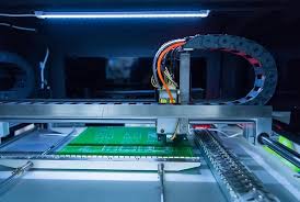
This article explores the various types of testing that are performed after quick turn pcb assembly, which includes bare board electrical testing, in-circuit testing (ICT), and automated optical inspection (AOI). These tests are designed to identify any flaws that may occur during production, such as soldering faults or debris on the board surface. During ICT, electrical probes are used to check for open and short circuits in the bare board, and can identify faults caused by poor soldering techniques, missing parts or incorrect component orientation. For larger or repeat batches, a test jig can be used to speed up the testing process.
Types of Testing That Are Performed After Quick Turn PCB Assembly
For bare boards that haven’t been printed with SMT components, a multi-point electrical test can be conducted using a flying probe or grid tester. The bare board’s conductivity is tested by applying different levels of current to designated points. This can be done with a power-on or power-off test, and is usually followed by a resistance of solvent extract (ROSE) test to determine the quality of the solder flux residue on the board’s copper plating, laminated structure and internal bonding surface.
The final phase of bare board electrical testing involves the use of a grid or flying probe test to verify the integrity of each pin of the bare board, and for continuity and isolation. A software program compares the net list against a known good board or master to ensure that all of the test points on the board are connected and have a minimum continuity resistance.
A AOI system can be added to the end of the PCB production line, or can be used with a sample of your bare board as a reference. The system uses single (2D) or dual (3D) cameras to take high-resolution images of your bare board and then compares them with the images of good and bad boards from a database to identify any flaws. This is a highly accurate and reliable method for identifying defects such as voids, excess or insufficient solder, surface scratches or debris on the bare board surface.