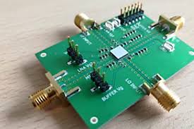
RF PCB Design
RF PCBs are the backbone of modern wireless communication devices, radar equipment, satellite technology and countless other applications that require the efficient transmission and reception of high-frequency signals. But to handle such signals with precision and efficiency, these circuit boards must meet specific design requirements and follow particular guidelines.
Unlike digital or analog signals, which are somewhat tolerant to poor impedance matching, RF and microwave signals demand higher tolerances. Moreover, rf pcb design must also account for additional factors such as crosstalk. This occurs when the signals in adjacent conductors interfere with each other, causing noise and interference. Fortunately, there are many ways to mitigate these problems.
One of the most important ways is by using decoupling or bypass conductors. This is a method of routing the signal return current paths so they don’t add to unwanted noise or impedance. Another way to reduce crosstalk is by minimizing the distance between signals. This can be done by incorporating DC decoupling.
Can RF PCB Design Be Recycled?
Another way to improve RF PCB performance is by routing the signals with proper impedance matching. This can be accomplished by utilizing microstrip or stripline transmission lines. In a microstrip transmission line, the signal trace is located on the top layer and the return path or ground plane is on the bottom. The characteristic impedance of the transmission line is determined by the thickness of the signal trace and the dielectric material.
Lastly, RF PCBs must address electromagnetic interference (EMI) and electromagnetic compatibility (EMC). This is a vital step to ensure that the RF signals don’t interfere with each other. This can be achieved by utilizing EMI shielding and filtering techniques.
It’s essential to keep in mind that a modular PCB layout makes it easier to disassemble and sort the components. This will help to speed up the recycling process and cut down on waste materials. It will also extend the lifespan of the board and allow for easy repair or upgrade. Additionally, using eco-friendly materials is vital for a sustainable future.
PCB recycling is a crucial part of the circular economy, which aims to create a closed-loop system in which resources are recycled and reused. However, the success of this concept depends on the proper disposal and recovery of materials from e-waste. This includes the use of a range of technologies, including thermal and chemical methods, as well as proper disposal practices.
Ultimately, the best way to recycle a PCB is to minimize the amount of e-waste that ends up in landfills and incinerators. This will minimize the amount of toxic chemicals and solvents that bleed into soil and water. It’s also important to promote a culture of responsible e-waste disposal, which will make it possible for consumers to reuse and recycle their devices and spare the earth of unnecessary pollution. Finally, it’s crucial to educate consumers about the importance of responsible e-waste disposal and provide them with information on the best options for recycling their electronics.